If you’ve ever worked with high-speed electronics—whether designing a gaming console, a 5G base station, or a medical device with precise signal processing—you’ve likely heard the term “impedance matching” thrown around. At our PCB manufacturing facility, we see this come up almost every day, and it’s not just a technical buzzword: it’s one of the most critical, yet often misunderstood, factors that can make or break a product’s performance. Many designers assume that as long as their circuits connect properly, everything will work. But skip proper impedance matching, and you might end up with a product that’s slower, less reliable, or even fails entirely after deployment. PCB Manufacturing
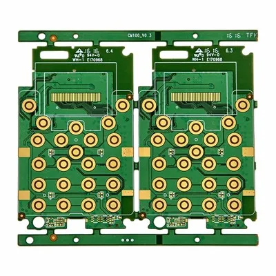
First, let’s ground this in a basic definition. Impedance is the total opposition a circuit presents to alternating current (AC) signals, measured in ohms. For DC signals, resistance is the primary concern, but for high-frequency signals (generally above 100MHz, though even lower frequencies matter for modern compact designs), impedance becomes dynamic. Impedance matching refers to aligning the impedance of your PCB’s signal traces, connectors, components, and the source driver to a consistent value—usually 50 ohms for general high-speed applications, 75 ohms for video and RF systems. When these values don’t align, the signal doesn’t flow cleanly from point A to point B; instead, some of it reflects back, creating a ripple effect that distorts the original signal.
Let’s break down why that reflection matters. Imagine your PCB is a highway, and a signal is a car driving at 100 km/h. If every few kilometers, the road narrows to a dirt path or widens into a field, the car has to slow down, swerve, or even stop. That sudden change in the road is exactly what impedance mismatch does to a high-frequency signal. The reflected signal bounces back toward the source, overlapping with the original signal and creating what’s called “signal ringing.” Ringing might look like small voltage spikes on an oscilloscope, but in real-world use, it can cause timing errors in microprocessors, corrupt data transfers, or even damage sensitive components. For example, in high-speed SerDes (Serializer/Deserializer) links used in 5G infrastructure or data centers, a 10% impedance mismatch can reduce signal integrity enough to drop entire data packets, leading to dropped calls or network outages.
Another less obvious consequence is signal attenuation. When a signal reflects, the portion that doesn’t reach its destination loses energy, so you end up with a weaker, less reliable signal. For long traces—say, a 10-inch trace on a high-speed graphics card PCB—attenuation can mean the signal arrives too weak for the receiver to interpret correctly. Designers sometimes try to compensate with stronger drivers, but that wastes power, generates more heat, and doesn’t fix the root problem of mismatch. At our shop, we’ve seen this firsthand: a client once brought in a prototype where a 15-inch trace had unaccounted-for impedance variation, and their initial tests showed data corruption at 1Gbps. By adjusting the trace width and dielectric thickness to hit a consistent 50 ohms, we fixed the issue, and they were able to run their signal at 2.5Gbps without errors.
Impedance matching also plays a huge role in electromagnetic interference (EMI). When a signal reflects, it creates unwanted electromagnetic radiation that can bleed into neighboring traces or devices. In products like wearables or IoT sensors, where space is tight and components are packed closely, this EMI can disrupt adjacent circuits—for example, a Bluetooth module interfering with a heart rate monitor sensor. Properly matched traces reduce reflection, so signals stay contained within their intended paths, cutting down on EMI and making your product easier to certify for regulatory standards like FCC, CE, or RoHS. Skipping impedance matching here often means costly re-designs or failed compliance tests down the line.
Now, how do we, as a PCB manufacturer, make sure impedance matching is done right? It’s not just a one-time step we check off; it’s a collaboration that starts with the design phase. First, we work with designers to understand their signal frequency, trace length, and target impedance. Then, we use our specialized impedance calculators—tools that account for the core material’s dielectric constant, trace width, trace thickness, and the distance between the trace and the ground plane. For example, a trace on a high-frequency Rogers material (common for RF designs) will have a different impedance than a trace on standard FR-4, because Rogers has a lower, more consistent dielectric constant. We also account for things like solder mask, which can add a tiny amount of capacitance to the trace, so we adjust our calculations to compensate.
But even with accurate calculations, manufacturing variables can throw impedance off. That’s why we maintain strict quality controls throughout production. We use automated optical inspection (AOI) to check trace widths to within 0.005mm, and we test a sample of every production run with time-domain reflectometry (TDR) — a method that sends a test signal down the trace and measures reflections to confirm impedance stays within ±5% of the target. This is non-negotiable for us; we’ve had clients reject entire batches before because their in-house testing found impedance variations, so we built our process to catch those issues before the boards leave our facility.
It’s important to note that impedance matching isn’t just for high-frequency designs anymore. Even for lower-speed digital circuits, like those in a modern smartwatch, impedance mismatch can cause issues. As components get smaller and signals get faster—today’s microcontrollers often run at hundreds of MHz—what was once a “low-speed” signal now behaves like a high-frequency one. We’ve seen clients come to us with old designs that worked on their 10-year-old PCBs but fail on new ones, simply because they didn’t adjust for the increased signal speed and smaller trace dimensions that affect impedance.
Another common myth: some designers think that matching only matters for long traces. But even short traces can cause problems if the frequency is high enough. A 2-inch trace carrying a 1GHz signal will still have impedance concerns, because the wavelength of a 1GHz signal is 300mm, so the trace is a significant fraction of that wavelength. A change in impedance over that short distance can lead to reflection, just like a long trace. That’s why we work closely with designers to check every trace, regardless of length, for their specific application.
Let’s talk about a real-world example that stuck with us. A few years ago, a startup came to us with a medical device: a portable glucose monitor that transferred data to a smartphone via Bluetooth. Their initial PCB design had a Bluetooth module trace with a 75-ohm target impedance, but they used a standard trace width calculation that didn’t account for the board’s thin dielectric (0.2mm) and the proximity of a power trace nearby. The result? The Bluetooth signal was dropping out 50% of the time when the device was near a phone. We adjusted the Bluetooth trace width to 0.12mm, modified the ground plane around the trace to avoid impedance changes from the power trace, and retested. The Bluetooth connection stayed solid, and the device passed all its clinical trials. That’s the impact proper impedance matching can have on a product that affects people’s lives.
Now, you might be wondering: how do I know if my design needs impedance matching? If your product has: high-speed digital signals (above 100MHz), RF or wireless components, long traces (over 1 inch), or requires data integrity for applications like gaming, industrial controls, or medical devices, then yes, you need to prioritize impedance matching. Even if you’re not sure, we can help. Our team works with designers at every stage, from initial layout to final manufacturing, to advise on impedance requirements.
At the end of the day, impedance matching is about ensuring your signal arrives at its destination exactly as it left the source. It’s a foundational step that prevents costly rework, reduces product failures, and helps your product meet performance and regulatory standards. Skipping it might seem like a way to save time or money upfront, but it almost always leads to bigger problems later—delay in product launches, lost revenue, or damage to your brand’s reputation.

If you’re designing a new PCB, troubleshooting a failed prototype, or want to ensure your next production run has perfect signal integrity, we’re here to help. Our team has years of experience in manufacturing PCBs for high-speed, RF, and medical applications, and we prioritize impedance matching at every step of the process. We work with you to understand your specific needs, adjust our manufacturing processes to hit your target impedance, and test every board to ensure quality. Reach out to us to discuss your project, and let’s make sure your next PCB design performs exactly as intended.
Rigid Flex PCB References
- Johnson, H., & Graham, M. (2003). High-Speed Signal Integrity. Prentice Hall.
- Bogatin, E. (2010). Signal Integrity Simplified. Prentice Hall.
- IPC-2141, Requirements for High-Speed Impedance Controlled Circuits. Association Connecting Electronics Industries.
- Rogers Corporation. (2022). High-Frequency Materials for Impedance Controlled Circuits. Technical Note TN-001.
Huaswin Electronics Technology Co., Ltd.
With abundant experience, we are one of the most professional pcb manufacturing manufacturers and suppliers in China. Welcome to wholesale customized pcb manufacturing at competitive price from our factory. If you have any enquiry about pricelist, please feel free to email us.
Address: Building A2, Hao Hai Hong Industrial Park, No.3 Yu He Road, Gong He, Sha Jing, Bao An, Shenzhen
E-mail: sales@huaswin.com
WebSite: https://www.huaswin-pcba.com/
